|
поискавой системы для электроныых деталей |
|
|
поискавой системы для электроныых деталей |
|
ML61 датащи(PDF) 6 Page - Minilogic Device Corporation Limited |
|
|
|||||||||||||||||||||||||||||
ML61 датащи(HTML) 6 Page - Minilogic Device Corporation Limited |
|
|
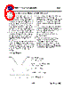
6 / 13 page  P6/13 Rev. H, August 2009 ML61 Functional Description (Refers to CMOS Output) 1. Firstly, when a voltage, higher than the Release Voltage (VDR) , is applied to the Voltage Input pin (VIN), that voltage will gradually fall. When a voltage higher than the Detect Voltage (VDF) is applied to the Input Voltage pin (VIN), output at VOUT will be equal to the input at the VIN pin. High impedance exists on the Output pin (VOUT) with the N-channel open drain configuration. If the pin is pulled-up. VOUT will be identical to the pull-up voltage. 2. When the input Voltage (VIN) falls below the Detect Voltage (VDF) level, the Output Voltage (VOUT) is equal to the Ground Voltage (VSS) level (detect state). Also applicable to N-channel open drain configuration. 3. When the Input Voltage (VIN) falls below the Minimum Operating Voltage (VMIN) level, output becomes unstable. In the case of N-channel open drain configuration, as the output pin is generally pulled-up, the output will be equal to the pull-up voltage. 4. When the Input Voltage (VIN) rises, output become stable once the voltage has exceeded VMIN. The Output Voltage (VOUT) will remain equal to the Ground Voltage (VSS) level until the Input Voltage (VIN) reaches the Detect Release Voltage (VDR) level. 5. When the Input Voltage (VIN) rises above the Detect Release Voltage (VDR) level, output at the Output pin (VOUT) is equal to VIN. (High impedance exists with the N-channel open drain output configuration and VOUT follows the pull-up voltage.) Notes : 1. The difference between VDR and VDF represents the Hysteresis Range. 2. The Propagation Delay Time (tDLY) represents the time it takes for the Input Voltage (VIN) to appear at the Output pin (VOUT), once the said voltage has exceeded the Release Voltage (VDR) level. Timing Diagram |
|
|
ссылки URL |
| Вашему бизинису помогли Аллдатащит? [ DONATE ] |
Что такое Аллдатащит | реклама | контакт | Конфиденциальность | Ссылка на техническое описание | обмен ссыками | поиск по производителю All Rights Reserved©Alldatasheet.com |
| Russian : Alldatasheetru.com | Korean : Alldatasheet.co.kr | Spanish : Alldatasheet.es | French : Alldatasheet.fr | Italian : Alldatasheetit.com Portuguese : Alldatasheetpt.com | Polish : Alldatasheet.pl | Vietnamese : Alldatasheet.vn Indian : Alldatasheet.in | Mexican : Alldatasheet.com.mx | British : Alldatasheet.co.uk | New Zealand : Alldatasheet.co.nz |
|
Family Site : ic2ic.com |
icmetro.com |
 Russian ▼
 English
 Chinese
 German
 Japanese
 Russian
 Korean
 Spanish
 French
 Italian
 Portuguese
 Polish
 Vietnamese
 Indian
 Mexican
 British
 New Zealand