|
поискавой системы для электроныых деталей |
|
|
поискавой системы для электроныых деталей |
|
OP467ARC/883 датащи(PDF) 14 Page - Analog Devices |
|
|
|||||||||||||||||||||||||||||
OP467ARC/883 датащи(HTML) 14 Page - Analog Devices |
|
|
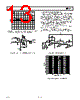
14 / 16 page  OP467 REV. C –14– FAST I-TO-V CONVERTER The fast slew rate and fast settling time of the OP467 are well suited to the fast buffers and I-to-V converters used in variety of applications. The circuit in Figure 46 is a unipolar quad D/A converter consisting of only two ICs. The current output of the DAC8408 is converted to a voltage by the OP467 configured as an I-to-V converter. This circuit is capable of settling to 0.1% within 200 ns. Figures 47 and 48 show the full-scale settling time of the outputs. To obtain reliable circuit performance, keep the traces from the DAC’s IOUT to the inverting inputs of the OP467 short to minimize parasitic capacitance. 10 0% 100 90 260.0ns 2V 50mV 100ns Figure 47. Voltage Output Settling Time 15 VDD VREFA RFBA IOUT 1A IOUT 2A/ IOUT 2B IOUT 1B RFBB VREFB DGND RFBC IOUT 1C IOUT 2C/ IOUT 2D VREFC IOUT 1D RFBD VREFD DAC8408 +5V +10V +10V VOUTA VOUTB 0.1 F +15V –15V C2 10pF C1 10pF 0.1 F 7 OP467 5 4 11 6 OP467 2 3 1 1 2 3 7 8 9 10 11 12 4 5 6 13 14 + +10V +10V VOUTA VOUTB DIGITAL CONTROL SIGNALS C3 10pF C4 10pF 14 12 13 OP467 DB0 (LSB) DB1 DB2 DB3 DB4 DB5 8 10 9 OP467 (MSB) DB7 DB6 28 27 26 22 21 20 19 18 17 25 24 23 16 + + – + – R/ W A/ B DS1 DS2 Figure 46. Quad DAC Unipolar Operation 10 0% 100 90 251.0ns 2V 50mV 100ns Figure 48. Voltage Output Settling Time RFB IOUT 3pF OP467 I-V DAC-8408 1k 50 604 60.4 2k DC OFFSET 2k AD847 Figure 49. DAC VOUT Settling Time Circuit |
|
|
ссылки URL |
| Вашему бизинису помогли Аллдатащит? [ DONATE ] |
Что такое Аллдатащит | реклама | контакт | Конфиденциальность | Ссылка на техническое описание | обмен ссыками | поиск по производителю All Rights Reserved©Alldatasheet.com |
| Russian : Alldatasheetru.com | Korean : Alldatasheet.co.kr | Spanish : Alldatasheet.es | French : Alldatasheet.fr | Italian : Alldatasheetit.com Portuguese : Alldatasheetpt.com | Polish : Alldatasheet.pl | Vietnamese : Alldatasheet.vn Indian : Alldatasheet.in | Mexican : Alldatasheet.com.mx | British : Alldatasheet.co.uk | New Zealand : Alldatasheet.co.nz |
|
Family Site : ic2ic.com |
icmetro.com |
 Russian ▼
 English
 Chinese
 German
 Japanese
 Russian
 Korean
 Spanish
 French
 Italian
 Portuguese
 Polish
 Vietnamese
 Indian
 Mexican
 British
 New Zealand