|
поискавой системы для электроныых деталей |
|
|
поискавой системы для электроныых деталей |
|
AMP01AX/883C датащи(PDF) 11 Page - Analog Devices |
|
|
|||||||||||||||||||||||||||||
AMP01AX/883C датащи(HTML) 11 Page - Analog Devices |
|
|
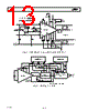
11 / 22 page  AMP01 –11– REV. D GAIN The AMP01 uses two external resistors for setting voltage gain over the range 0.1 to 10,000. The magnitudes of the scale resis- tor, RS, and gain-set resistor, RG, are related by the formula: G = 20 × R S/RG, where G is the selected voltage gain (refer to Figure 29). REFERENCE OUTPUT V+ V– RS RG +IN –IN VOLTAGE GAIN, G = 20 RS RG ( ) SENSE AMP01 14 15 13 12 7 9 8 11 10 3 2 1 18 Figure 29. Basic AMP01 Connections for Gains 0.1 to 10,000 The magnitude of RS affects linearity and output referred errors. Circuit performance is characterized using RS = 10 k Ω when operating on ±15 volt supplies and driving a ±10 volt output. R S may be reduced to 5 k Ω in many applications particularly when operating on ±5 volt supplies or if the output voltage swing is limited to ±5 volts. Bandwidth is improved with R S = 5 k Ω and this also increases common-mode rejection by approximately 6 dB at low gain. Lowering the value below 5 k Ω can cause instability in some circuit configurations and usually has no advantage. High voltage gains between two and ten thousand would require very low values of RG. For RS = 10 k Ω and AV = 2000 we get RG = 100 Ω; this value is the practical lower limit for RG. Below 100 Ω, mismatch of wirebond and resistor temperature coefficients will introduce significant gain tempco errors. Therefore, for gains above 2,000, RG should be kept constant at 100 Ω and R S increased. The maximum gain of 10,000 is obtained with RS set to 50 k Ω. Metal-film or wirewound resistors are recommended for best results. The absolute values and TCs are not too important, only the ratiometric parameters. AC amplifiers require good gain stability with temperature and time, but dc performance is unimportant. Therefore, low cost metal-film types with TCs of 50 ppm/ °C are usually adequate for RS and RG. Realizing the full potential of the AMP01’s offset voltage and gain stability requires precision metal-film or wire- wound resistors. Achieving a 15 ppm/ °C gain tempco at all gains requires RS and RG temperature coefficient matching to 5 ppm/ °C or better. INPUT AND OUTPUT OFFSET VOLTAGES Instrumentation amplifiers have independent offset voltages associated with the input and output stages. While the initial offsets may be adjusted to zero, temperature variations will cause shifts in offsets. Systems with auto-zero can correct for offset errors, so initial adjustment would be unnecessary. How- ever, many high-gain applications don’t have auto zero. For these applications, both offsets can be nulled, which has mini- mal effect on TCVIOS and TCVOOS The input offset component is directly multiplied by the ampli- fier gain, whereas output offset is independent of gain. There- fore, at low gain, output-offset errors dominate, while at high gain, input-offset errors dominate. Overall offset voltage, VOS, referred to the output (RTO) is calculated as follows; VOS (RTO) = (VIOS × G) + V OOS (1) where VIOS and VOOS are the input and output offset voltage specifications and G is the amplifier gain. Input offset nulling alone is recommended with amplifiers having fixed gain above 50. Output offset nulling alone is recommended when gain is fixed at 50 or below. In applications requiring both initial offsets to be nulled, the input offset is nulled first by short-circuiting RG, then the output offset is nulled with the short removed. The overall offset voltage drift TCVOS, referred to the output, is a combination of input and output drift specifications. Input offset voltage drift is multiplied by the amplifier gain, G, and summed with the output offset drift; TCVOS (RTO) = (TCVIOS × G) + TCV OOS (2) where TCVIOS is the input offset voltage drift, and TCVOOS is the output offset voltage specification. Frequently, the amplifier drift is referred back to the input (RTI), which is then equiva- lent to an input signal change; TCVOS (RTI) = TCVIOS TCV OOS G (3) For example, the maximum input-referred drift of an AMP01 EX set to G = 1000 becomes; TCVOS (RTI ) = 0.3 µV/°C + 100 1000 µVC / ° = 0.4 µV/°C max INPUT BIAS AND OFFSET CURRENTS Input transistor bias currents are additional error sources that can degrade the input signal. Bias currents flowing through the signal source resistance appear as an additional offset voltage. Equal source resistance on both inputs of an IA will minimize offset changes due to bias current variations with signal voltage and temperature. However, the difference between the two bias currents, the input offset current, produces a nontrimmable error. The magnitude of the error is the offset current times the source resistance. A current path must always be provided between the differential inputs and analog ground to ensure correct amplifier operation. Floating inputs, such as thermocouples, should be grounded close to the signal source for best common-mode rejection. |
|
|
ссылки URL |
| Вашему бизинису помогли Аллдатащит? [ DONATE ] |
Что такое Аллдатащит | реклама | контакт | Конфиденциальность | Ссылка на техническое описание | обмен ссыками | поиск по производителю All Rights Reserved©Alldatasheet.com |
| Russian : Alldatasheetru.com | Korean : Alldatasheet.co.kr | Spanish : Alldatasheet.es | French : Alldatasheet.fr | Italian : Alldatasheetit.com Portuguese : Alldatasheetpt.com | Polish : Alldatasheet.pl | Vietnamese : Alldatasheet.vn Indian : Alldatasheet.in | Mexican : Alldatasheet.com.mx | British : Alldatasheet.co.uk | New Zealand : Alldatasheet.co.nz |
|
Family Site : ic2ic.com |
icmetro.com |
 Russian ▼
 English
 Chinese
 German
 Japanese
 Russian
 Korean
 Spanish
 French
 Italian
 Portuguese
 Polish
 Vietnamese
 Indian
 Mexican
 British
 New Zealand