|
поискавой системы для электроныых деталей |
|
|
поискавой системы для электроныых деталей |
|
AD8231ACPZ-R7 датащи(PDF) 8 Page - Analog Devices |
|
|
|||||||||||||||||||||||||||||
AD8231ACPZ-R7 датащи(HTML) 8 Page - Analog Devices |
|
|
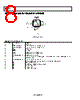
8 / 24 page  AD8231 Rev. A | Page 8 of 24 PIN CONFIGURATION AND FUNCTION DESCRIPTIONS PIN 1 INDICATOR 1 NC 2 (IN-AMP –IN) –INA 3 (IN-AMP +IN) +INA 4 NC 11 –VS 12 +VS 10 OUTA (IN-AMP OUT) 9REF TOP VIEW (Not to Scale) AD8231 NC = NO CONNECT Figure 2. Pin Configuration Table 6. Pin Function Descriptions Pin Number Mnemonic Description 1 NC No Connect. 2 −INA (IN-AMP −IN) Instrumentation Amplifier Negative Input. 3 +INA (IN-AMP +IN) Instrumentation Amplifier Positive Input. 4 NC No Connect. 5 SDN Shutdown. 6 +INB Operational Amplifier Positive Input. 7 −INB Operational Amplifier Negative Input. 8 OUTB (OP AMP OUT) Operational Amplifier Output. 9 REF Instrumentation Amplifier Reference Pin. It should be driven with a low impedance. Output is referred to this pin. 10 OUTA (IN-AMP OUT) Instrumentation Amplifier Output. 11 −VS Negative Power Supply. Connect to ground in single-supply applications. 12 +VS Positive Power Supply. 13 CS Chip Select. Enables digital logic interface. 14 A0 Gain Setting Bit (LSB). 15 A1 Gain Setting Bit. 16 A2 Gain Setting Bit (MSB). |
|
|
ссылки URL |
| Вашему бизинису помогли Аллдатащит? [ DONATE ] |
Что такое Аллдатащит | реклама | контакт | Конфиденциальность | Ссылка на техническое описание | обмен ссыками | поиск по производителю All Rights Reserved©Alldatasheet.com |
| Russian : Alldatasheetru.com | Korean : Alldatasheet.co.kr | Spanish : Alldatasheet.es | French : Alldatasheet.fr | Italian : Alldatasheetit.com Portuguese : Alldatasheetpt.com | Polish : Alldatasheet.pl | Vietnamese : Alldatasheet.vn Indian : Alldatasheet.in | Mexican : Alldatasheet.com.mx | British : Alldatasheet.co.uk | New Zealand : Alldatasheet.co.nz |
|
Family Site : ic2ic.com |
icmetro.com |
 Russian ▼
 English
 Chinese
 German
 Japanese
 Russian
 Korean
 Spanish
 French
 Italian
 Portuguese
 Polish
 Vietnamese
 Indian
 Mexican
 British
 New Zealand