|
поискавой системы для электроныых деталей |
|
|
поискавой системы для электроныых деталей |
|
MAX5500AGAP+ датащи(PDF) 7 Page - Maxim Integrated Products |
|
|
|||||||||||||||||||||||||||||
MAX5500AGAP+ датащи(HTML) 7 Page - Maxim Integrated Products |
|
|
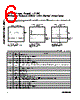
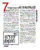
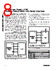
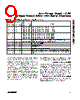
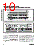
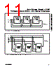
7 / 15 page  Low-Power, Quad, 12-Bit Voltage-Output DACs with Serial Interface _______________________________________________________________________________________ 7 Detailed Description The MAX5500/MAX5501 integrate four 12-bit, voltage- output digital-to-analog converters (DACs) that are addressed through a simple 3-wire serial interface. The devices include a 16-bit data-in/data-out shift register. Each internal DAC provides a doubled-buffered input composed of an input register and a DAC register (see the Functional Diagram). The negative input of each amplifier is externally accessible. The DACs are inverted rail-to-rail ladder networks that convert 12-bit digital inputs into equivalent analog out- put voltages in proportion to the applied reference volt- age inputs. DACs A and B share the REFAB input, while DACs C and D share the REFCD input. The two reference inputs allow different full-scale output voltage ranges for each pair of DACs. Figure 1 shows a simpli- fied circuit diagram of one of the four DACs. Reference Inputs The two reference inputs accept positive DC and AC signals. The voltage at each reference input sets the full-scale output voltage for the two corresponding DACs. The reference input voltage range is 0V to (VDD - 1.4V). The output voltages (VOUT_) are represented by a digitally programmable voltage source as: VOUT_ = (VREF x NB/4096) x Gain where NB is the numeric value of the binary input code (0 to 4095) of the DAC. VREF is the reference voltage. Gain is the externally set voltage gain. The impedance at each reference input is code-depen- dent, ranging from a low value of 10kΩ when both DACs connected to the reference accept an input code of 555 hex, to a high value exceeding giga-ohms with an input code of 000 hex. The load regulation of the ref- erence source affects the performance of the devices as the input impedance at the reference inputs is code dependent. The REFAB and REFCD reference inputs provide a 10kΩ guaranteed minimum input impedance. When the same voltage source drives the two reference inputs, the effective minimum impedance is 5kΩ. A volt- age reference with an excellent load regulation of 0.0002mV/mA, such as the MAX6033, is capable of dri- ving both reference inputs simultaneously at 2.5V. Driving REFAB and REFCD separately improves refer- ence accuracy. The REFAB and REFCD inputs enter a high-impedance state, with a typical input leakage current of 0.02µA, when the MAX5500/MAX5501 are in shutdown. The ref- erence input capacitance is also code dependent and typically ranges from 20pF with an input code of all 0s to 100pF with an input code of all 1s. Output Amplifiers All DAC outputs are internally buffered by precision amplifiers with a typical slew rate of 0.6V/µs. Access to the inverting input of each output amplifier provides the greater flexibility in output gain setting/signal condition- ing (see the Applications Information section). With a full-scale transition at the output, the typical set- tling time to within ±0.5 LSB is 12µs when the output is loaded with 5kΩ in parallel with 100pF. A load of less than 2kΩ at the output degrades performance. See the Typical Operating Characteristics for the output dynamic responses and settling performances of the amplifiers. Power-Down Mode The MAX5500/MAX5501 feature a software-program- mable shutdown that reduces supply current to a typi- cal value of 10µA. Drive PDL high to enable the shutdown mode. Write 1100XXXXXXXXXXXX as the input-control word to put the device in power-down mode (Table 1). In power-down mode, the output amplifiers and the ref- erence inputs enter a high-impedance state. The serial interface remains active. Data in the input registers is retained in power-down, allowing the devices to recall the output states prior to entering shut- down. Start up from power-down either by recalling the previous configuration or by updating the DACs with new data. Allow 15µs for the outputs to stabilize when powering up the devices or bringing the devices out of shutdown. OUT_ FB_ SHOWN FOR ALL 1s ON DAC D0 D9 D10 D11 2R 2R 2R 2R 2R RR R REF_ AGND Figure 1. Simplified DAC Circuit Diagram |
|
|
ссылки URL |
| Вашему бизинису помогли Аллдатащит? [ DONATE ] |
Что такое Аллдатащит | реклама | контакт | Конфиденциальность | Ссылка на техническое описание | обмен ссыками | поиск по производителю All Rights Reserved©Alldatasheet.com |
| Russian : Alldatasheetru.com | Korean : Alldatasheet.co.kr | Spanish : Alldatasheet.es | French : Alldatasheet.fr | Italian : Alldatasheetit.com Portuguese : Alldatasheetpt.com | Polish : Alldatasheet.pl | Vietnamese : Alldatasheet.vn Indian : Alldatasheet.in | Mexican : Alldatasheet.com.mx | British : Alldatasheet.co.uk | New Zealand : Alldatasheet.co.nz |
|
Family Site : ic2ic.com |
icmetro.com |
 Russian ▼
 English
 Chinese
 German
 Japanese
 Russian
 Korean
 Spanish
 French
 Italian
 Portuguese
 Polish
 Vietnamese
 Indian
 Mexican
 British
 New Zealand