|
поискавой системы для электроныых деталей |
|
|
поискавой системы для электроныых деталей |
|
USBDF02W5 датащи(PDF) 4 Page - STMicroelectronics |
|
|
|||||||||||||||||||||||||||||
USBDF02W5 датащи(HTML) 4 Page - STMicroelectronics |
|
|
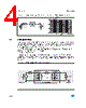
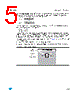
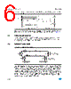
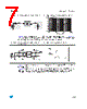
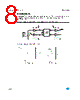
4 / 11 page  Application information USBDFxxW5 4/11 2.2 ESD protection In addition to the requirements of termination and EMC compatibility, computing devices are required to be tested for ESD susceptibility. This test is described in the IEC 61000-4-2 and is already in place in Europe. This test requires that a device tolerates ESD events and remain operational without user intervention. The USBDFxxW5 is particularly optimized to perform ESD protection. ESD protection is based on the use of device which clamps at : This protection function is split in 2 stages. As shown in Figure 5., the ESD strikes are clamped by the first stage S1 and then the remaining overvoltage is applied to the second stage through the resistor R. Such a configuration makes the output voltage very low at the Vout level. Figure 5. USBDFxxW5 ESD clamping behavior Figure 3. Measurement configuration Figure 4. USBDFxxW5 attenuation curve 50 Ω RF IN Vg 50 Ω TG OUT TEST BOARD 1 10 100 1000 3000 -30 -20 -10 0 F (MHz) Insertion loss (dB) V= V + R .I INPUT BR d pp ESD Surge Vinput Voutput Rload Rg R S1 Rd V BR V BR V PP Device to be protected USBDFxxW5 Rd S2 |
|
|
ссылки URL |
| Вашему бизинису помогли Аллдатащит? [ DONATE ] |
Что такое Аллдатащит | реклама | контакт | Конфиденциальность | Ссылка на техническое описание | обмен ссыками | поиск по производителю All Rights Reserved©Alldatasheet.com |
| Russian : Alldatasheetru.com | Korean : Alldatasheet.co.kr | Spanish : Alldatasheet.es | French : Alldatasheet.fr | Italian : Alldatasheetit.com Portuguese : Alldatasheetpt.com | Polish : Alldatasheet.pl | Vietnamese : Alldatasheet.vn Indian : Alldatasheet.in | Mexican : Alldatasheet.com.mx | British : Alldatasheet.co.uk | New Zealand : Alldatasheet.co.nz |
|
Family Site : ic2ic.com |
icmetro.com |
 Russian ▼
 English
 Chinese
 German
 Japanese
 Russian
 Korean
 Spanish
 French
 Italian
 Portuguese
 Polish
 Vietnamese
 Indian
 Mexican
 British
 New Zealand