|
поискавой системы для электроныых деталей |
|
|
поискавой системы для электроныых деталей |
|
ADMV1455BBCZ-R7 датащи(PDF) 68 Page - Analog Devices |
|
|
|||||||||||||||||||||||||||||
ADMV1455BBCZ-R7 датащи(HTML) 68 Page - Analog Devices |
|
|
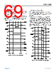
68 / 141 page  Data Sheet ADMV1455 THEORY OF OPERATION analog.com Rev. 0 | 68 of 141 Initialization SPI Instructions Starting at tINITIALIZE (see Figure 167), configure the chip by using the SPI instructions for its intended operation. Give all the neces- sary SPI instructions to configure the chip, looping from tINITIALIZE to the ready time, tREADY for each instruction. Keep the CEN input low during the initialization SPI instructions, and complete the initialization at tREADY. Chip Enable and Operation After all the initialization SPI instructions have been completed, wait a minimum of t16 to ensure that the digital logic has processed the instructions prior to setting the CEN input high at tOPERATIONAL to enable chip operation. At tOPERATIONAL, the RF portions of the chip are enabled. See Figure 168 for more information. During chip operation, any necessary SPI instructions can be giv- en, along with the LOAD input toggles, and any changes to the ADD_Fx and ADD_Gx inputs. Continue operating, looping from tOPERATIONAL to tCONTINUE until it is desired to either disable the chip, reset the chip, or power down the chip. Figure 168. Operational Timing Diagram |
|
ссылки URL |
| Вашему бизинису помогли Аллдатащит? [ DONATE ] |
Что такое Аллдатащит | реклама | контакт | Конфиденциальность | Ссылка на техническое описание | обмен ссыками | поиск по производителю All Rights Reserved©Alldatasheet.com |
| Russian : Alldatasheetru.com | Korean : Alldatasheet.co.kr | Spanish : Alldatasheet.es | French : Alldatasheet.fr | Italian : Alldatasheetit.com Portuguese : Alldatasheetpt.com | Polish : Alldatasheet.pl | Vietnamese : Alldatasheet.vn Indian : Alldatasheet.in | Mexican : Alldatasheet.com.mx | British : Alldatasheet.co.uk | New Zealand : Alldatasheet.co.nz |
|
Family Site : ic2ic.com |
icmetro.com |
 Russian ▼
 English
 Chinese
 German
 Japanese
 Russian
 Korean
 Spanish
 French
 Italian
 Portuguese
 Polish
 Vietnamese
 Indian
 Mexican
 British
 New Zealand