|
поискавой системы для электроныых деталей |
|
|
поискавой системы для электроныых деталей |
|
CDC536DB датащи(PDF) 4 Page - Texas Instruments |
|
|
|||||||||||||||||||||||||||||
CDC536DB датащи(HTML) 4 Page - Texas Instruments |
|
|
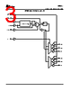
4 / 16 page  www.ti.com ABSOLUTE MAXIMUM RATINGS CDC536 SCAS378G – APRIL 1994 – REVISED JULY 2004 FUNCTIONAL BLOCK DIAGRAM (continued) Terminal Functions TERMINAL I/O DESCRIPTION NAME NO. Clock input. CLKIN provides the clock signal to be distributed by the CDC536 clock-driver circuit. CLKIN is used to provide the reference signal to the integrated phase-lock loop that generates the clock output CLKIN 3 I signals. CLKIN must have a fixed frequency and fixed phase in order for the phase-lock loop to obtain phase lock. Once the circuit is powered up and a valid CLKIN signal is applied, a stabilization time is required for the phase-lock loop to phase lock the feedback signal to its reference signal. CLR 24 I CLR is used for testing purposes only. Connect CLR to GND for normal operation. Feedback input. FBIN provides the feedback signal to the internal PLL. FBIN must be hardwired to one of FBIN 26 I the six clock outputs to provide frequency and phase lock. The internal PLL adjusts the output clocks to obtain zero phase delay between the FBIN and differential CLKIN inputs. Output enable. OE is the output enable for all outputs. When OE is low, all outputs are enabled. When OE is high, all outputs are in the high-impedance state. Since the feedback signal for the phase-lock loop is OE 5 I taken directly from an output, placing the outputs in the high-impedance state interrupts the feedback loop; therefore, when a high-to-low transition occurs at OE, enabling the output buffers, a stabilization time is required before the phase-lock loop obtains phase lock. Output configuration select. SEL selects the output configuration for each output bank (e.g. 1 ×, 1/2×, or SEL 4 I 2 ×).(see Tables 1 and 2). TEST is used to bypass the phase-lock loop circuitry for factory testing of the device. When TEST is low, TEST 25 I all outputs operate using the PLL circuitry. When TEST is high, the outputs are placed in a test mode that bypasses the PLL circuitry. TEST should be grounded for normal operation. These outputs are configured by SEL to transmit one-half or one-fourth the frequency of the VCO. The 1Y1-1Y3 7, 10, 13 O relationship between the CLKIN frequency and the output frequency is dependent on SEL. The duty cycle of the Y output signals is nominally 50%, independent of the duty cycle of the CLKIN signal. These outputs transmit one-half the frequency of the VCO. The relationship between the CLKIN frequency 2Y1-2Y3 22, 19, 16 O and the output frequency is dependent on the frequency of the output being fed back to FBIN. The duty cycle of the Y output signals is nominally 50% independent of the duty cycle of the CLKIN signal. over operating free-air temperature range (unless otherwise noted)(1) UNIT Supply voltage range, VCC -0.5 V to 4.6 V Input voltage range, VI (see (2)) -0.5 V to 7 V Voltage range applied to any output in the high state or power-off state, VO(see (2)) -0.5 V to 5.5 V Current into any output in the low state, IO 64 mA Input clamp current, IIK(VI < 0) -20 mA Output clamp current, IOK(VO < 0) -50 mA Maximum power dissipation at TA = 55°C (in still air) (see (3)): DB package 0.68 W DL package 0.7 W Operating free-air temperature range, TA 0 °C to 70°C Storage temperature range, Tstg -65 °C to 150°C (1) Stresses beyond those listed under "absolute maximum ratings” may cause permanent damage to the device. These are stress ratings only, and functional operation of the device at these or any other conditions beyond those indicated under "recommended operating conditions” is not implied. Exposure to absolute-maximum-rated conditions for extended periods may affect device reliability. (2) The input and output negative-voltage ratings may be exceeded if the input and output clamp-current ratings are observed. (3) The maximum package power dissipation is calculated using a junction temperature of 150 °C and a board trace length of 75 mils. For more information, refer to the Package Thermal Considerations application note in the ABT Advanced BiCMOS Technology Data Book, literature number SCBD002. 4 |
|
|
ссылки URL |
| Вашему бизинису помогли Аллдатащит? [ DONATE ] |
Что такое Аллдатащит | реклама | контакт | Конфиденциальность | Ссылка на техническое описание | обмен ссыками | поиск по производителю All Rights Reserved©Alldatasheet.com |
| Russian : Alldatasheetru.com | Korean : Alldatasheet.co.kr | Spanish : Alldatasheet.es | French : Alldatasheet.fr | Italian : Alldatasheetit.com Portuguese : Alldatasheetpt.com | Polish : Alldatasheet.pl | Vietnamese : Alldatasheet.vn Indian : Alldatasheet.in | Mexican : Alldatasheet.com.mx | British : Alldatasheet.co.uk | New Zealand : Alldatasheet.co.nz |
|
Family Site : ic2ic.com |
icmetro.com |
 Russian ▼
 English
 Chinese
 German
 Japanese
 Russian
 Korean
 Spanish
 French
 Italian
 Portuguese
 Polish
 Vietnamese
 Indian
 Mexican
 British
 New Zealand