|
поискавой системы для электроныых деталей |
|
|
поискавой системы для электроныых деталей |
|
ADA4700-1ARDZ-R7 датащи(PDF) 23 Page - Analog Devices |
|
|
|||||||||||||||||||||||||||||
ADA4700-1ARDZ-R7 датащи(HTML) 23 Page - Analog Devices |
|
|
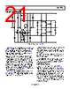
23 / 28 page  Data Sheet ADA4700-1 DRIVING CAPACITIVE LOADS Although the ADA4700-1 behaves well when driving capacitive loads, CL, as seen in Figure 27 to Figure 30, extra compensation can improve the response when large capacitances need to be accommodated. The simplest way of accomplishing this is with a snubber network, as shown in Figure 61. Figure 61. Snubber Network For unity-gain applications and capacitive loads up to 1 nF, RSNUB = 150 Ω and CSNUB = 10 nF works well. Results for this circuit are shown in Figure 64. With higher closed-loop gains, lighter snubbing can be used. For capacitive loads up to 10 nF, the snubber must be larger. Figure 65 shows the results of using an RSNUB = 22 Ω, CSNUB = 100 nF, and CL = 10 nF with the ADA4700-1 in a gain of 10. Because the snubber network places an ac load on the amplifier, snubbing does not work well when larger capacitive loads are used, or when large transients are present. A better approach is to use a bypass network in the feedback path, as shown in Figure 62. Figure 62. Unity-Gain Configuration with Bypass Network The bypass network in Figure 62 performs well with loads up to 100 nF. The resulting waveforms are shown in Figure 66 for various output amplitudes. For heavier loads, capacitive feedback, CFB, must be increased. The configuration in Figure 62 can be modified to work with gains greater than 1. Figure 63 shows a bypass network with a gain of 10 system, and results for various output amplitudes are shown in Figure 67. Figure 63. Bypass Network with Gain of 10 System Figure 64. Results from Snubber Network with AV = +1 and CL = 10 pF to 1 nF Figure 65. Results from Snubber Network with Higher Gains, CL = 10 nF Figure 66. Results of Bypass Network for Various Output Amplitudes, Unity Gain with CL = 100 nF RSNUB VOUT VIN CSNUB CL VOUT VIN 3.3kΩ 22Ω 10nF CFB CL VOUT VIN 3.3kΩ CFB 5.1kΩ 43kΩ 22Ω CL –10 –8 –6 –4 –2 0 2 4 6 8 10 0 2 4 6 8 10 12 14 TIME (µs) OUTPUT INPUT VSY = ±50V AV = +1 CL = 10pF TO 1nF –15 –10 –5 0 5 10 15 0 0.2 0.4 0.6 0.8 TIME (ms) 1.0 1.2 1.4 VSY = ±50V AV = +10 CL = 10nF –10 –8 –6 –4 –2 0 2 4 6 8 10 0 0.2 0.4 0.6 TIME (ms) 0.8 1.0 1.2 VSY = ±50V AV = +1 CL = 100nF Rev. 0 | Page 23 of 28 |
|
ссылки URL |
| Вашему бизинису помогли Аллдатащит? [ DONATE ] |
Что такое Аллдатащит | реклама | контакт | Конфиденциальность | Ссылка на техническое описание | обмен ссыками | поиск по производителю All Rights Reserved©Alldatasheet.com |
| Russian : Alldatasheetru.com | Korean : Alldatasheet.co.kr | Spanish : Alldatasheet.es | French : Alldatasheet.fr | Italian : Alldatasheetit.com Portuguese : Alldatasheetpt.com | Polish : Alldatasheet.pl | Vietnamese : Alldatasheet.vn Indian : Alldatasheet.in | Mexican : Alldatasheet.com.mx | British : Alldatasheet.co.uk | New Zealand : Alldatasheet.co.nz |
|
Family Site : ic2ic.com |
icmetro.com |
 Russian ▼
 English
 Chinese
 German
 Japanese
 Russian
 Korean
 Spanish
 French
 Italian
 Portuguese
 Polish
 Vietnamese
 Indian
 Mexican
 British
 New Zealand