|
поискавой системы для электроныых деталей |
|
|
поискавой системы для электроныых деталей |
|
ADL5532ACPZ-R7 датащи(PDF) 5 Page - Analog Devices |
|
|
|||||||||||||||||||||||||||||
ADL5532ACPZ-R7 датащи(HTML) 5 Page - Analog Devices |
|
|
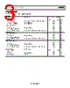
5 / 8 page  Preliminary Technical Data ADL5532 Rev. PrD 5/07 | Page 5 of 8 PIN CONFIGURATION AND FUNCTION DESCRIPTIONS 5CLIN 8FBK2 NC 4 6NC RFIN 2 7RFOUT NC 3 FBK 1 PIN 1 INDICATOR TOP VIEW (Not to Scale) ADL5532 Figure 2. Pin Configuration Table 3. Pin Function Descriptions Single Pin No. Mnemonic Description 1,8 FBK1, FBK2 For operation below 50 MHz a 100nF capacitor should be connected between these pins. 2 RFIN RF Input: Requires a DC blocking capacitor. For normal operating conditions a 10 nF capacitor is recommended 7 RFOUT RF Output and Bias: DC bias provided to this pin through an inductor. For normal operating conditions a 470 nH inductor is recommended. RF path requires a DC blocking capacitor. For normal operating conditions a 10 nF capacitor is recommended. 3, 4, 6 NC No Connect 5 CLIN A 100 nF capacitor connected between pin 5 and ground provides decoupling for the on board linearizer. Exposed Paddle Internally connected to GND. Solder to a low impedance ground plane |
|
|
ссылки URL |
| Вашему бизинису помогли Аллдатащит? [ DONATE ] |
Что такое Аллдатащит | реклама | контакт | Конфиденциальность | Ссылка на техническое описание | обмен ссыками | поиск по производителю All Rights Reserved©Alldatasheet.com |
| Russian : Alldatasheetru.com | Korean : Alldatasheet.co.kr | Spanish : Alldatasheet.es | French : Alldatasheet.fr | Italian : Alldatasheetit.com Portuguese : Alldatasheetpt.com | Polish : Alldatasheet.pl | Vietnamese : Alldatasheet.vn Indian : Alldatasheet.in | Mexican : Alldatasheet.com.mx | British : Alldatasheet.co.uk | New Zealand : Alldatasheet.co.nz |
|
Family Site : ic2ic.com |
icmetro.com |
 Russian ▼
 English
 Chinese
 German
 Japanese
 Russian
 Korean
 Spanish
 French
 Italian
 Portuguese
 Polish
 Vietnamese
 Indian
 Mexican
 British
 New Zealand