|
поискавой системы для электроныых деталей |
|
|
поискавой системы для электроныых деталей |
|
AS7225 датащи(PDF) 67 Page - OSRAM GmbH |
|
|
|||||||||||||||||||||||||||||
AS7225 датащи(HTML) 67 Page - OSRAM GmbH |
|
|
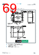
67 / 76 page  Document Feedback AS7225 Application Information Datasheet • PUBLIC DS000496 • v2-00 • 2019-Jun-28 75 │ 66 13.3 PCB Pad Layout Suggested PCB pad layout guidelines for the LGA package are shown. Flash Gold is recommended as a surface finish for the landing pads. Figure 90: Recommended PCB Pad Layout (Top View) (1) Unless otherwise specified, all dimensions are in millimeters. (2) Add 0.05 mm all around the nominal lead width and length for the PCB pad land pattern. (3) This drawing is subject to change without notice. |
|
ссылки URL |
| Вашему бизинису помогли Аллдатащит? [ DONATE ] |
Что такое Аллдатащит | реклама | контакт | Конфиденциальность | Ссылка на техническое описание | обмен ссыками | поиск по производителю All Rights Reserved©Alldatasheet.com |
| Russian : Alldatasheetru.com | Korean : Alldatasheet.co.kr | Spanish : Alldatasheet.es | French : Alldatasheet.fr | Italian : Alldatasheetit.com Portuguese : Alldatasheetpt.com | Polish : Alldatasheet.pl | Vietnamese : Alldatasheet.vn Indian : Alldatasheet.in | Mexican : Alldatasheet.com.mx | British : Alldatasheet.co.uk | New Zealand : Alldatasheet.co.nz |
|
Family Site : ic2ic.com |
icmetro.com |
 Russian ▼
 English
 Chinese
 German
 Japanese
 Russian
 Korean
 Spanish
 French
 Italian
 Portuguese
 Polish
 Vietnamese
 Indian
 Mexican
 British
 New Zealand