|
поискавой системы для электроныых деталей |
|
|
поискавой системы для электроныых деталей |
|
AD628ARMZ-R7 датащи(PDF) 16 Page - Analog Devices |
|
|
|||||||||||||||||||||||||||||
AD628ARMZ-R7 датащи(HTML) 16 Page - Analog Devices |
|
|
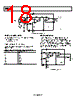
16 / 20 page  AD628 Rev. F | Page 16 of 20 The differential input voltage range is constrained to the linear operation of the internal amplifiers A1 and A2. The voltage applied to the inputs of A1 and A2 should be between VS− + 1.2 V and VS+ − 1.2 V. Similarly, the outputs of A1 and A2 should be kept between VS− + 0.9 V and VS+ − 0.9 V. VOLTAGE LEVEL CONVERSION Industrial signal conditioning and control applications typically require connections between remote sensors or amplifiers and centrally located control modules. Signal conditioners provide output voltages of up to ±10 V full scale. However, ADCs or microprocessors operating on single 3.3 V to 5 V logic supplies are now the norm. Thus, the controller voltages require further reduction in amplitude and reference. Furthermore, voltage potentials between locations are seldom compatible, and power line peaks and surges can generate destructive energy between utility grids. The AD628 offers an ideal solution to both problems. It attenuates otherwise destruc- tive signal voltage peaks and surges by a factor of 10 and shifts the differential input signal to the desired output voltage. Conversion from voltage-driven or current-loop systems is easily accomplished using the circuit shown in Figure 32. This shows a circuit for converting inputs of various polarities and amplitudes to the input of a single-supply ADC. To adjust common-mode output voltage, connect Pin 3 (VREF) and the lower end of the 10 kΩ resistor to the desired voltage. The output common-mode voltage is the same as the reference voltage. Designing such an application can be done in a few simple steps, including the following: • Determine the required gain. For example, if the input voltage must be transformed from ±10 V to 0 V to +5 V, the gain is +5/+20 or +0.25. • Determine if the circuit common-mode voltage should be changed. An AD7940 ADC is illustrated for this example. When operating from a 5 V supply, the common-mode voltage of the AD7940 is half the supply, or 2.5 V. If the AD628 reference pin and the lower terminal of the 10 kΩ resistor are connected to a 2.5 V voltage source, the output common-mode voltage is 2.5 V. Table 6 shows resistor and reference values for commonly used single-supply converter voltages. REXT3 is included as an option to balance the source impedance into A2. This is described in more detail in the Gain Adjustment section. Table 6. Nearest 1% Resistor Values for Voltage Level Conversion Applications Input Voltage (V) ADC Supply Voltage (V) Desired Output Voltage (V) VREF (V) REXT1 (kΩ) REXT2 (kΩ) ±10 5 2.5 2.5 15 10 ±5 5 2.5 2.5 39.7 10 10 5 2.5 0 39.7 10 5 5 2.5 0 89.8 10 ±10 3 1.25 1.25 2.49 10 ±5 3 1.25 1.25 15 10 10 3 1.25 0 15 10 5 3 1.25 0 39.7 10 |
|
|
ссылки URL |
| Вашему бизинису помогли Аллдатащит? [ DONATE ] |
Что такое Аллдатащит | реклама | контакт | Конфиденциальность | Ссылка на техническое описание | обмен ссыками | поиск по производителю All Rights Reserved©Alldatasheet.com |
| Russian : Alldatasheetru.com | Korean : Alldatasheet.co.kr | Spanish : Alldatasheet.es | French : Alldatasheet.fr | Italian : Alldatasheetit.com Portuguese : Alldatasheetpt.com | Polish : Alldatasheet.pl | Vietnamese : Alldatasheet.vn Indian : Alldatasheet.in | Mexican : Alldatasheet.com.mx | British : Alldatasheet.co.uk | New Zealand : Alldatasheet.co.nz |
|
Family Site : ic2ic.com |
icmetro.com |
 Russian ▼
 English
 Chinese
 German
 Japanese
 Russian
 Korean
 Spanish
 French
 Italian
 Portuguese
 Polish
 Vietnamese
 Indian
 Mexican
 British
 New Zealand