|
поискавой системы для электроныых деталей |
|
|
поискавой системы для электроныых деталей |
|
TLV751 датащи(PDF) 3 Page - Texas Instruments |
|
|
|
|||||||||||||||||||||||||||||
TLV751 датащи(HTML) 3 Page - Texas Instruments |
|
|
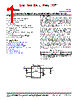
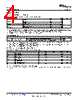
3 / 29 page  1 FB1 2 GND 3 EN1 4 GND 5 EN2 6 IN1 7 FB2 8 OUT1 9 IN2 10 OUT2 Not to scale Thermal Pad 3 TLV751 www.ti.com SBVS385 – DECEMBER 2019 Product Folder Links: TLV751 Submit Documentation Feedback Copyright © 2019, Texas Instruments Incorporated 5 Pin Configuration and Functions DSQ Package 10-Pin Adjustable WSON Top View Pin Functions PIN I/O DESCRIPTION NAME DSQ EN1 3 Input Enable pin. Drive EN1 greater than VEN1(HI) to turn on the regulator. Drive EN1 less than VEN1(LO) to put the low-dropout (LDO) regulator into shutdown mode. EN2 5 Input Enable pin. Drive EN2 greater than VEN2(HI) to turn on the regulator. Drive EN2 less than VEN2(LO) to put the LDO into shutdown mode. FB1 1 — This pin is used as an input to the control loop error amplifier and is used to set the output voltage of the LDO. FB2 7 — This pin is used as an input to the control loop error amplifier and is used to set the output voltage of the LDO. GND 2, 4 — Ground pin IN1 6 Input Input pin. For best transient response and to minimize input impedance, use the recommended value or larger ceramic capacitor from IN to ground; see the Recommended Operating Conditions table and the Input and Output Capacitor Selection section. Place the input capacitor as close to the output of the device as possible. IN2 9 Input Input pin. For best transient response and to minimize input impedance, use the recommended value or larger ceramic capacitor from IN to ground; see the Recommended Operating Conditions table and the Input and Output Capacitor Selection section. Place the input capacitor as close to the output of the device as possible. OUT1 8 Output Regulated output voltage pin. A capacitor is required from OUT to ground for stability. For best transient response, use the nominal recommended value or larger ceramic capacitor from OUT to ground; see the Recommended Operating Conditions table and the Input and Output Capacitor Selection section. Place the output capacitor as close to output of the device as possible. OUT2 10 Output Regulated output voltage pin. A capacitor is required from OUT to ground for stability. For best transient response, use the nominal recommended value or larger ceramic capacitor from OUT to ground; see the Recommended Operating Conditions table and the Input and Output Capacitor Selection section. Place the output capacitor as close to output of the device as possible. Thermal pad Pad — Connect the thermal pad to a large area GND plane for improved thermal performance. |
|
ссылки URL |
| Вашему бизинису помогли Аллдатащит? [ DONATE ] |
Что такое Аллдатащит | реклама | контакт | Конфиденциальность | Ссылка на техническое описание | обмен ссыками | поиск по производителю All Rights Reserved©Alldatasheet.com |
| Russian : Alldatasheetru.com | Korean : Alldatasheet.co.kr | Spanish : Alldatasheet.es | French : Alldatasheet.fr | Italian : Alldatasheetit.com Portuguese : Alldatasheetpt.com | Polish : Alldatasheet.pl | Vietnamese : Alldatasheet.vn Indian : Alldatasheet.in | Mexican : Alldatasheet.com.mx | British : Alldatasheet.co.uk | New Zealand : Alldatasheet.co.nz |
|
Family Site : ic2ic.com |
icmetro.com |
 Russian ▼
 English
 Chinese
 German
 Japanese
 Russian
 Korean
 Spanish
 French
 Italian
 Portuguese
 Polish
 Vietnamese
 Indian
 Mexican
 British
 New Zealand