|
поискавой системы для электроныых деталей |
|
|
поискавой системы для электроныых деталей |
|
AAT2510 датащи(PDF) 2 Page - Advanced Analogic Technologies |
|
|
|||||||||||||||||||||||||||||
AAT2510 датащи(HTML) 2 Page - Advanced Analogic Technologies |
|
|
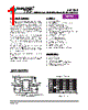
2 / 20 page  Pin Descriptions Pin Configuration TDFN33-12 (Top View) EN1 FB1 SGND1 1 EN2 FB2 SGND2 VIN1 LX1 GND1 VIN2 LX2 GND2 2 3 4 5 6 12 11 10 9 8 7 Pin # Symbol Function 1, 4 EN1, EN2 Converter enable input. A logic high enables the converter channel. A logic low forces the channel into shutdown mode, reducing the channel supply current to less than 1µA. This pin should not be left floating. When not actively controlled, this pin can be tied directly to the source voltage (VIN1, VIN2). 2, 5 FB1, FB2 Feedback input pin. For fixed output voltage versions, this pin is connected to the converter output, forcing the converter to regulate to the specified voltage. For adjustable versions, an external resistive divider ties to this point and programs the output voltage to the desired value. 3, 6 SGND1, SGND2 Signal ground. For external feedback, return the feedback resistive divider to this ground. For internal fixed version, tie to the point of load return. See section on PCB layout guidelines and evaluation board layout diagram. 7, 10 GND2, GND1 Main power ground return. Connect to the input and output capacitor return. See sec- tion on PCB layout guidelines and evaluation board layout diagram. 8, 11 LX2, LX1 Output switching node that connects to the respective output inductor. 9, 12 VIN2, VIN1 Input supply voltage. Must be closely decoupled to the respective power gnd. EP Exposed paddle (bottom). Use properly sized vias for thermal coupling to the ground plane. See section on PCB layout guidelines. AAT2510 Dual 400mA, 1MHz Step-Down DC-DC Converter 2 2510.2005.08.1.5 |
|
|
ссылки URL |
| Вашему бизинису помогли Аллдатащит? [ DONATE ] |
Что такое Аллдатащит | реклама | контакт | Конфиденциальность | Ссылка на техническое описание | обмен ссыками | поиск по производителю All Rights Reserved©Alldatasheet.com |
| Russian : Alldatasheetru.com | Korean : Alldatasheet.co.kr | Spanish : Alldatasheet.es | French : Alldatasheet.fr | Italian : Alldatasheetit.com Portuguese : Alldatasheetpt.com | Polish : Alldatasheet.pl | Vietnamese : Alldatasheet.vn Indian : Alldatasheet.in | Mexican : Alldatasheet.com.mx | British : Alldatasheet.co.uk | New Zealand : Alldatasheet.co.nz |
|
Family Site : ic2ic.com |
icmetro.com |
 Russian ▼
 English
 Chinese
 German
 Japanese
 Russian
 Korean
 Spanish
 French
 Italian
 Portuguese
 Polish
 Vietnamese
 Indian
 Mexican
 British
 New Zealand