 |
поискавой системы для электроныых деталей |
|
|
поискавой системы для электроныых деталей |
|
The question interval is too short.
Please try again in a few seconds.

Hello, Please ask a question about 93LC46BT-E/MS Datasheet
# Example questions:
➢ What happens if a start bit is issued and then cs is taken low? how does this affect the do pin?
➢ What voltage must vcc be for the erase all (eral) instruction to function correctly?
➢ How does the initiation of the self-timed auto-erase and programming cycle differ between the '93aa/93lc' devices and the '93c' devices when performing a 'write' operation?
| Part No. | 93LC46BT-E/MS |
| Manufacturer | MICROCHIP |
| Size | 403 Kbytes |
| Pages | 24 pages |
| Description | 1K Microwire Compatible Serial EEPROM |

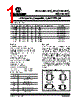


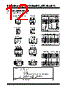




hybridization between these two, ensuring a comprehensive understanding. Let's break this down into sections focusing on key areas: Memory Organization, Command Set, Timing Characteristics, Protection Mechanisms, and Additional Notes.
1. Memory Organization
️· Density & Architecture: The 93XX46A/B/C family are SPI EEPROMs. SPI means Serial Peripheral Interface - they communicate using a simple serial data bus.
️· Organization: The document mentions sizes like "entire memory array," suggesting these are typically larger capacity devices. The 'A', 'B', and 'C' variants imply different configurations or feature sets.
️· Word Size: The data is written in bytes (8 bits) or words (16 bits), depending on the device configuration and whether the ORG (Organization) pin is high or low. This determines if you've got an 8-bit or 16-bit device.
️· Addressability: Each memory location is uniquely addressable, allowing for both individual byte/word writes and mass erase/write operations.
2. Command Set
The document details a set of commands controlling the EEPROM's behavior. Here’s a breakdown:
️· ERASE (Instruction): Erases a specific memory location (or the entire array with `ERAL`). Requires CS low, followed by falling edge of CS to initiate the write cycle (except on 93C devices which require rising edge of CLK).
️· ERAL (Erase All): Erase the *entire* memory array. Similar timing to `ERASE`. Requires CS low, falling edge of CS on 93AA/LC, rising edge of CLK on 93C.
️· EWDS (Erase/Write Disable): Disables all programming commands. The device powers up in this mode.
️· EWEN (Erase/Write Enable): Enables programming commands. Required *before* `ERASE` or `WRITE` operations.
️· READ: Outputs the data from a specific memory location. A dummy zero precedes the data.
️· WRITE: Writes data to a specific memory location. CS must go low to trigger the write cycle.
️· WRAL (Write All): Writes data to the *entire* memory array. Automatically includes an `ERAL` cycle. A successor to `ERAL`.
3. Timing Characteristics (Crucial for Integration)
️· TCSL (Chip Select Low Time): A minimum time (250 ns) that CS must be low for commands to execute.
️· TPD (Output Delay): The delay between clocking in data and the data appearing on the output (DO) pin during a `READ` operation.
️· Timing Differences (AA/LC vs. C): Significant differences exist between the 'AA/LC' (93AA46A/B/C and 93LC46A/B/C) devices and the 'C' (93C46A/B/C) devices regarding the triggering of write cycles. The 'AA/LC' devices use the falling edge of CS, while the 'C' devices use the rising edge of CLK. *This is a key point to avoid errors.*
️· Sequential Read: Supports reading data sequentially without re-issuing commands.
4. Protection Mechanisms
️· VCC Protection: Operation is inhibited if VCC is below a threshold voltage (1.5V for 'AA' and 'LC', 3.8V for 'C').
️· EWDS/EWEN: Provides a software-controlled mechanism to disable/enable programming, preventing accidental writes.
️· READ Independence: The READ operation is not affected by the EWDS/EWEN status.
️· Data Protection The `EWDS` instruction provides additional protection against accidental programming during normal operation.
5. Additional Notes
️· ORG (Organization Pin): The ORG pin determines whether the device operates in 8-bit or 16-bit mode. This impacts the size of data being read and written.
️· Dummy Zero: A dummy zero bit is output during `READ` operations.
️· Ready/Busy Status: The DO pin provides a READY/BUSY status indicator during erase and write cycles.
️· SPI Interface: The EEPROM uses a serial peripheral interface for communication, keeping the pin count low and simplifying integration.
️· HALT Command - Not specifically mentioned, but SPI EEPROMs often have a "HALT" command to pause ongoing operations.
Key Takeaways & Potential Integration Challenges
️· Device Variation: The differences between the "AA/LC" and "C" devices are significant, particularly concerning write cycle triggering. Careful design is needed to handle these variations.
️· Timing Sensitivity: SPI interfaces are timing-sensitive. Careful attention to clock speed, setup/hold times, and CS timing is crucial for reliable operation.
️· Ready/Busy Handling: The Ready/Busy status is vital for integrating the EEPROM into larger systems. Proper handling of this status prevents data corruption and ensures correct operation.
️· HALT Command Considerations: If your design requires the ability to pause ongoing operations, consider implementing the HALT command.
hybridization between these two, ensuring a comprehensive understanding. Let's break this down into sections focusing on key areas: Memory Organization, Command Set, Timing Characteristics, Protection Mechanisms, and Additional Notes.
1. Memory Organization
️· Density & Architecture: The 93XX46A/B/C family are SPI EEPROMs. SPI means Serial Peripheral Interface - they communicate using a simple serial data bus.
️· Organization: The document mentions sizes like "entire memory array," suggesting these are typically larger capacity devices. The 'A', 'B', and 'C' variants imply different configurations or feature sets.
️· Word Size: The data is written in bytes (8 bits) or words (16 bits), depending on the device configuration and whether the ORG (Organization) pin is high or low. This determines if you've got an 8-bit or 16-bit device.
️· Addressability: Each memory location is uniquely addressable, allowing for both individual byte/word writes and mass erase/write operations.
2. Command Set
The document details a set of commands controlling the EEPROM's behavior. Here’s a breakdown:
️· ERASE (Instruction): Erases a specific memory location (or the entire array with `ERAL`). Requires CS low, followed by falling edge of CS to initiate the write cycle (except on 93C devices which require rising edge of CLK).
️· ERAL (Erase All): Erase the *entire* memory array. Similar timing to `ERASE`. Requires CS low, falling edge of CS on 93AA/LC, rising edge of CLK on 93C.
️· EWDS (Erase/Write Disable): Disables all programming commands. The device powers up in this mode.
️· EWEN (Erase/Write Enable): Enables programming commands. Required *before* `ERASE` or `WRITE` operations.
️· READ: Outputs the data from a specific memory location. A dummy zero precedes the data.
️· WRITE: Writes data to a specific memory location. CS must go low to trigger the write cycle.
️· WRAL (Write All): Writes data to the *entire* memory array. Automatically includes an `ERAL` cycle. A successor to `ERAL`.
3. Timing Characteristics (Crucial for Integration)
️· TCSL (Chip Select Low Time): A minimum time (250 ns) that CS must be low for commands to execute.
️· TPD (Output Delay): The delay between clocking in data and the data appearing on the output (DO) pin during a `READ` operation.
️· Timing Differences (AA/LC vs. C): Significant differences exist between the 'AA/LC' (93AA46A/B/C and 93LC46A/B/C) devices and the 'C' (93C46A/B/C) devices regarding the triggering of write cycles. The 'AA/LC' devices use the falling edge of CS, while the 'C' devices use the rising edge of CLK. *This is a key point to avoid errors.*
️· Sequential Read: Supports reading data sequentially without re-issuing commands.
4. Protection Mechanisms
️· VCC Protection: Operation is inhibited if VCC is below a threshold voltage (1.5V for 'AA' and 'LC', 3.8V for 'C').
️· EWDS/EWEN: Provides a software-controlled mechanism to disable/enable programming, preventing accidental writes.
️· READ Independence: The READ operation is not affected by the EWDS/EWEN status.
️· Data Protection The `EWDS` instruction provides additional protection against accidental programming during normal operation.
5. Additional Notes
️· ORG (Organization Pin): The ORG pin determines whether the device operates in 8-bit or 16-bit mode. This impacts the size of data being read and written.
️· Dummy Zero: A dummy zero bit is output during `READ` operations.
️· Ready/Busy Status: The DO pin provides a READY/BUSY status indicator during erase and write cycles.
️· SPI Interface: The EEPROM uses a serial peripheral interface for communication, keeping the pin count low and simplifying integration.
️· HALT Command - Not specifically mentioned, but SPI EEPROMs often have a "HALT" command to pause ongoing operations.
Key Takeaways & Potential Integration Challenges
️· Device Variation: The differences between the "AA/LC" and "C" devices are significant, particularly concerning write cycle triggering. Careful design is needed to handle these variations.
️· Timing Sensitivity: SPI interfaces are timing-sensitive. Careful attention to clock speed, setup/hold times, and CS timing is crucial for reliable operation.
️· Ready/Busy Handling: The Ready/Busy status is vital for integrating the EEPROM into larger systems. Proper handling of this status prevents data corruption and ensures correct operation.
️· HALT Command Considerations: If your design requires the ability to pause ongoing operations, consider implementing the HALT command.
| Part No. | 93LC46BT-E/MS |
| Manufacturer | MICROCHIP |
| Size | 403 Kbytes |
| Pages | 24 pages |
| Description | 1K Microwire Compatible Serial EEPROM |
| Вашему бизинису помогли Аллдатащит? [ DONATE ] |
Что такое Аллдатащит | реклама | контакт | Конфиденциальность | Ссылка на техническое описание | обмен ссыками | поиск по производителю All Rights Reserved©Alldatasheet.com |
| Russian : Alldatasheetru.com | Korean : Alldatasheet.co.kr | Spanish : Alldatasheet.es | French : Alldatasheet.fr | Italian : Alldatasheetit.com Portuguese : Alldatasheetpt.com | Polish : Alldatasheet.pl | Vietnamese : Alldatasheet.vn Indian : Alldatasheet.in | Mexican : Alldatasheet.com.mx | British : Alldatasheet.co.uk | New Zealand : Alldatasheet.co.nz |
|
Family Site : ic2ic.com |
icmetro.com |
 Russian ▼
  English
 Chinese
 German
 Japanese
 Korean
 Spanish
 French
 Italian
 Portuguese
 Polish
 Vietnamese
 Indian
 Mexican
 British
 New Zealand