 |
поискавой системы для электроныых деталей |
|
|
поискавой системы для электроныых деталей |
|
The question interval is too short.
Please try again in a few seconds.

Hello, Please ask a question about IXFA24N60X Datasheet
# Example questions:
➢ What generally happens to the stored energy in the output capacitance as the drain-source voltage (vds) increases?
➢ From the rds(on) limit graph (last image), what happens to the resistance as the current increases?
➢ Examine figure 14. what does the graph tell you about the thermal impedance of the device during a short-duration pulse compared to a longer-duration pulse?
| Part No. | IXFA24N60X |
| Manufacturer | IXYS |
| Size | 160 Kbytes |
| Pages | 6 pages |
| Description | Preliminary Technical Information |


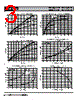


1. Device Identification & General Information:
️· Device Name (Likely): 24N60X(J6) - This is indicated at the very bottom, and consistent with the content. It suggests a 24 Amp, 600V MOSFET.
️· Manufacturer: IXYS Corporation
️· Revision: F\_24N60X(J6) 5-20-15-A – Indicates a revision date.
️· Statement: "IXYS Reserves the Right to Change Limits, Test Conditions, and Dimensions" - Standard disclaimer in datasheets.
2. Electrical Characteristics (This is by far the most extensive part - it's difficult to present all data precisely without interactive tables, but I've captured highlights):
️· Voltage Ratings: Likely a 600V device, though this is not explicitly stated. A maximum transient voltage is shown on some graphs.
️· Current Ratings: "24" Ampere is referenced somewhere, indicating a significant current handling capacity.
️· RDS(on): "RDS(on) Limit" is shown, likely with multiple values for different gate voltages.
️· Input Capacitance (Ciss): Represented in graphs.
️· Output Capacitance (Coss): Represented in graphs.
️· Reverse Transfer Capacitance (Crss): Represented in graphs.
️· Gate Charge (Qg): Shown with multiple values for different gate voltages.
️· Forward Voltage Drop of Intrinsic Diode: Graph showing a typical value around 0.8-1.1V.
️· Threshold Voltage (Vgs(th)): (Not explicitly shown, but implied to be a typical value).
️· Breakdown Voltage (BVdss): (Not explicitly shown, likely around 600V).
3. Characteristics Graphs & Plots (Description of key graphs, these are harder to describe fully without interactive visuals):
️· Fig. 2: Safe Operating Area (SOA) – Maximum Ratings: Shows maximum current vs. voltage under various temperature conditions. Important for understanding how to avoid device failure.
️· Fig. 3: Output Characteristics: Shows current (ID) vs. voltage (VDS) for different gate voltages. A standard way to visualize device performance.
️· Fig. 4: Transfer Characteristics: Shows gate-source voltage (VGS) vs. drain current (ID) for different gate-source voltages.
️· Fig. 8: Forward Voltage Drop of Intrinsic Diode: Shows a typical diode forward voltage characteristic.
️· Fig. 11: Capacitance: Shows capacitance (Ciss, Coss, Crss) vs. voltage (VDS).
️· Fig. 13: Output Capacitance Stored Energy: Shows stored energy vs. voltage, useful for transient circuit design.
️· Fig. 14: Maximum Transient Thermal Impedance: Crucial for thermal management - shows how the device's thermal resistance changes over time.
4. Additional Notes / Details from Graphs:
️· Single Pulse: Some graphs have an annotation "Single Pulse" – indicating the data is relevant to brief, high-power events.
️· TJ Temperature: References to Junction Temperature (TJ). Monitoring TJ is essential to prevent overheating.
️· µ: The Greek letter "µ" is used – likely representing micro (10<sup>-6</sup>).
️· Ciss, Coss, Crss: Abbreviations for Input, Output, and Reverse Transfer Capacitances respectively.
Important Caveats & How to Use This Summary:
️· This is a text-based interpretation: Without seeing the actual images, some details are estimates based on typical MOSFET datasheets. The *exact* values and specifications would be in the full datasheet.
️· Datasheets are complex: This is a summary, not a replacement for the complete datasheet. You *must* consult the full datasheet for accurate specifications and design guidelines.
️· Design Considerations: MOSFET design requires careful attention to voltage, current, power dissipation, and thermal management.
️· Safety: Always observe safety precautions when working with power electronics.
1. Device Identification & General Information:
️· Device Name (Likely): 24N60X(J6) - This is indicated at the very bottom, and consistent with the content. It suggests a 24 Amp, 600V MOSFET.
️· Manufacturer: IXYS Corporation
️· Revision: F\_24N60X(J6) 5-20-15-A – Indicates a revision date.
️· Statement: "IXYS Reserves the Right to Change Limits, Test Conditions, and Dimensions" - Standard disclaimer in datasheets.
2. Electrical Characteristics (This is by far the most extensive part - it's difficult to present all data precisely without interactive tables, but I've captured highlights):
️· Voltage Ratings: Likely a 600V device, though this is not explicitly stated. A maximum transient voltage is shown on some graphs.
️· Current Ratings: "24" Ampere is referenced somewhere, indicating a significant current handling capacity.
️· RDS(on): "RDS(on) Limit" is shown, likely with multiple values for different gate voltages.
️· Input Capacitance (Ciss): Represented in graphs.
️· Output Capacitance (Coss): Represented in graphs.
️· Reverse Transfer Capacitance (Crss): Represented in graphs.
️· Gate Charge (Qg): Shown with multiple values for different gate voltages.
️· Forward Voltage Drop of Intrinsic Diode: Graph showing a typical value around 0.8-1.1V.
️· Threshold Voltage (Vgs(th)): (Not explicitly shown, but implied to be a typical value).
️· Breakdown Voltage (BVdss): (Not explicitly shown, likely around 600V).
3. Characteristics Graphs & Plots (Description of key graphs, these are harder to describe fully without interactive visuals):
️· Fig. 2: Safe Operating Area (SOA) – Maximum Ratings: Shows maximum current vs. voltage under various temperature conditions. Important for understanding how to avoid device failure.
️· Fig. 3: Output Characteristics: Shows current (ID) vs. voltage (VDS) for different gate voltages. A standard way to visualize device performance.
️· Fig. 4: Transfer Characteristics: Shows gate-source voltage (VGS) vs. drain current (ID) for different gate-source voltages.
️· Fig. 8: Forward Voltage Drop of Intrinsic Diode: Shows a typical diode forward voltage characteristic.
️· Fig. 11: Capacitance: Shows capacitance (Ciss, Coss, Crss) vs. voltage (VDS).
️· Fig. 13: Output Capacitance Stored Energy: Shows stored energy vs. voltage, useful for transient circuit design.
️· Fig. 14: Maximum Transient Thermal Impedance: Crucial for thermal management - shows how the device's thermal resistance changes over time.
4. Additional Notes / Details from Graphs:
️· Single Pulse: Some graphs have an annotation "Single Pulse" – indicating the data is relevant to brief, high-power events.
️· TJ Temperature: References to Junction Temperature (TJ). Monitoring TJ is essential to prevent overheating.
️· µ: The Greek letter "µ" is used – likely representing micro (10<sup>-6</sup>).
️· Ciss, Coss, Crss: Abbreviations for Input, Output, and Reverse Transfer Capacitances respectively.
Important Caveats & How to Use This Summary:
️· This is a text-based interpretation: Without seeing the actual images, some details are estimates based on typical MOSFET datasheets. The *exact* values and specifications would be in the full datasheet.
️· Datasheets are complex: This is a summary, not a replacement for the complete datasheet. You *must* consult the full datasheet for accurate specifications and design guidelines.
️· Design Considerations: MOSFET design requires careful attention to voltage, current, power dissipation, and thermal management.
️· Safety: Always observe safety precautions when working with power electronics.
| Part No. | IXFA24N60X |
| Manufacturer | IXYS |
| Size | 160 Kbytes |
| Pages | 6 pages |
| Description | Preliminary Technical Information |
| Вашему бизинису помогли Аллдатащит? [ DONATE ] |
Что такое Аллдатащит | реклама | контакт | Конфиденциальность | Ссылка на техническое описание | обмен ссыками | поиск по производителю All Rights Reserved©Alldatasheet.com |
| Russian : Alldatasheetru.com | Korean : Alldatasheet.co.kr | Spanish : Alldatasheet.es | French : Alldatasheet.fr | Italian : Alldatasheetit.com Portuguese : Alldatasheetpt.com | Polish : Alldatasheet.pl | Vietnamese : Alldatasheet.vn Indian : Alldatasheet.in | Mexican : Alldatasheet.com.mx | British : Alldatasheet.co.uk | New Zealand : Alldatasheet.co.nz |
|
Family Site : ic2ic.com |
icmetro.com |
 Russian ▼
  English
 Chinese
 German
 Japanese
 Korean
 Spanish
 French
 Italian
 Portuguese
 Polish
 Vietnamese
 Indian
 Mexican
 British
 New Zealand