 |
поискавой системы для электроныых деталей |
|
|
поискавой системы для электроныых деталей |
|
The question interval is too short.
Please try again in a few seconds.

Hello, Please ask a question about DTA114EKA Datasheet
# Example questions:
➢ What is the maximum allowable supply voltage for this dta144eka transistor?
➢ How does the input resistance (r1) typically compare to the resistance ratio (r2/r1)?
➢ What is the typical transition frequency (ft) of this transistor under the specified test conditions?
| Part No. | DTA114EKA |
| Manufacturer | LRC |
| Size | 76 Kbytes |
| Pages | 2 pages |
| Description | Digital transistors(built-in resistors) |

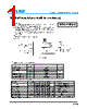


# DTA144EKA Digital Transistor
## Features
️· Built-in bias resistors simplify inverter circuit design (no external resistors needed).
️· Thin-film resistors provide isolation and minimize parasitic effects.
️· Easy operation requiring only on/off condition setting.
## Structure
PNP digital transistor with built-in resistors
## Absolute Maximum Ratings
️· Supply Voltage (Vcc): –50V
️· Input Voltage (Vin): –40V to +10V
️· Output Current (Io): –30mA
️· Output Current (Ic(Max)): -100mA
️· Power Dissipation (Pd): 200mW
️· Junction Temperature (Tj): 150°C
️· Storage Temperature (Tstg): –55°C to +150°C
## Electrical Characteristics (Ta = 25°C)
️· Input Voltage (V I(off)): –0.5V (Vcc = –5V, Io = –100µA)
️· Input Voltage (V I(on)): –3.0V (Vo= –0.3V, Io= –2mA)
️· Output Voltage (Vo(on)): –0.1 to –0.3V (Io/Ii = -10mA / -0.5mA)
️· Input Current (Ii): –0.18mA (Vi = –5V)
️· Output Current (Io(off)): –0.5µA (Vcc = –50V, Vi = 0V)
️· DC Current Gain (Gi): 68 (Vo = –5V, Io = –5mA)
️· Input Resistance (R1): 32.9 to 61.1 KΩ
️· Resistance Ratio (R2/R1): 0.8 to 1.2
️· Transition Frequency (fT): 250 MHz (Vce = -10V, Ie = 5mA, f=100MHz)
## Electrical Characteristic Curves
️· Figure 1: Input voltage vs. output current (ON characteristics)
️· Figure 2: Output current vs. input voltage (OFF characteristics)
️· Figure 3: DC current gain vs. output current
️· Figure 4: Output voltage vs. output current
# DTA144EKA Digital Transistor
## Features
️· Built-in bias resistors simplify inverter circuit design (no external resistors needed).
️· Thin-film resistors provide isolation and minimize parasitic effects.
️· Easy operation requiring only on/off condition setting.
## Structure
PNP digital transistor with built-in resistors
## Absolute Maximum Ratings
️· Supply Voltage (Vcc): –50V
️· Input Voltage (Vin): –40V to +10V
️· Output Current (Io): –30mA
️· Output Current (Ic(Max)): -100mA
️· Power Dissipation (Pd): 200mW
️· Junction Temperature (Tj): 150°C
️· Storage Temperature (Tstg): –55°C to +150°C
## Electrical Characteristics (Ta = 25°C)
️· Input Voltage (V I(off)): –0.5V (Vcc = –5V, Io = –100µA)
️· Input Voltage (V I(on)): –3.0V (Vo= –0.3V, Io= –2mA)
️· Output Voltage (Vo(on)): –0.1 to –0.3V (Io/Ii = -10mA / -0.5mA)
️· Input Current (Ii): –0.18mA (Vi = –5V)
️· Output Current (Io(off)): –0.5µA (Vcc = –50V, Vi = 0V)
️· DC Current Gain (Gi): 68 (Vo = –5V, Io = –5mA)
️· Input Resistance (R1): 32.9 to 61.1 KΩ
️· Resistance Ratio (R2/R1): 0.8 to 1.2
️· Transition Frequency (fT): 250 MHz (Vce = -10V, Ie = 5mA, f=100MHz)
## Electrical Characteristic Curves
️· Figure 1: Input voltage vs. output current (ON characteristics)
️· Figure 2: Output current vs. input voltage (OFF characteristics)
️· Figure 3: DC current gain vs. output current
️· Figure 4: Output voltage vs. output current
| Part No. | DTA114EKA |
| Manufacturer | LRC |
| Size | 76 Kbytes |
| Pages | 2 pages |
| Description | Digital transistors(built-in resistors) |
| Вашему бизинису помогли Аллдатащит? [ DONATE ] |
Что такое Аллдатащит | реклама | контакт | Конфиденциальность | Ссылка на техническое описание | обмен ссыками | поиск по производителю All Rights Reserved©Alldatasheet.com |
| Russian : Alldatasheetru.com | Korean : Alldatasheet.co.kr | Spanish : Alldatasheet.es | French : Alldatasheet.fr | Italian : Alldatasheetit.com Portuguese : Alldatasheetpt.com | Polish : Alldatasheet.pl | Vietnamese : Alldatasheet.vn Indian : Alldatasheet.in | Mexican : Alldatasheet.com.mx | British : Alldatasheet.co.uk | New Zealand : Alldatasheet.co.nz |
|
Family Site : ic2ic.com |
icmetro.com |
 Russian ▼
  English
 Chinese
 German
 Japanese
 Korean
 Spanish
 French
 Italian
 Portuguese
 Polish
 Vietnamese
 Indian
 Mexican
 British
 New Zealand