 |
поискавой системы для электроныых деталей |
|
|
поискавой системы для электроныых деталей |
|
The question interval is too short.
Please try again in a few seconds.

Hello, Please ask a question about AD8348_15 Datasheet
# Example questions:
➢ What is the typical maximum drive current for the vref pin?
➢ What is the purpose of the iofs and qofs pins, and how can they be used to improve the performance of the ad8348?
➢ What impedance should be presented to the loip and loin inputs for optimal performance, and how is this achieved?
| Part No. | AD8348_15 |
| Manufacturer | AD |
| Size | 929 Kbytes |
| Pages | 28 pages |
| Description | 50 MHz to 1000 MHz Quadrature Demodulator |

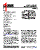


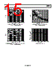
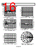
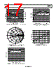


Okay, let's break down the information provided in this AD8348 datasheet excerpt. Here's a summary of the key points, organized for clarity:
1. Device Overview:
️· What it is: The AD8348 is a versatile mixer and baseband receiver/demodulator IC. It's designed for applications like direct-conversion receivers (zero-IF), heterodyne receivers, and more.
️· Functionality: It combines a high-performance mixer section with baseband amplifiers and offset nulling capabilities.
2. Pinout & Function Descriptions (Crucial for Usage):
️· Pin Count: 28-Lead TSSOP package.
️· Key Pins and their roles:
- LOIP, LOIN: Local Oscillator Inputs (for mixing). Requires a balun or matching network to achieve a 50Ω input impedance.
- VPOS1, VPOS2, VPOS3: Positive supply pins for the LO, IF and baseband circuits (need decoupling capacitors).
- IOPP, IOPN, QOPP, QOPN: I and Q-channel differential baseband outputs.
- VCMO: Baseband common-mode voltage control. Critical for setting the DC bias of outputs and inputs.
- IAIN, QAIN: I and Q-channel baseband amplifier inputs.
- IMXO, QMXO: I and Q-channel mixer outputs.
- IFIN, IFIP: Intermediate Frequency (IF) inputs.
- IOFS, QOFS: Offset nulling inputs for I and Q channels.
- VREF: Reference voltage output (1V). Used for bias.
3. Absolute Maximum Ratings (Important for Safety):
️· Supply Voltage: 5.5V
️· Input Power Limits: LO power: 10 dBm, IF power: 18 dBm.
️· Junction Temperature: 150°C (Stay below this!)
️· Operating Temperature Range: -40°C to +85°C.
️· Storage Temperature Range: -65°C to +125°C
4. Key Considerations & Recommendations:
️· Impedance Matching: Carefully match impedances, especially at the LO and IF inputs, to avoid signal reflections and maximize performance.
️· Decoupling: Decouple the power supply pins with capacitors (as noted in the pin descriptions).
️· DC Biasing: Understand how VCMO controls the DC bias of the baseband signals.
️· Offset Nulling: Use the IOFS and QOFS pins to minimize DC offsets.
In essence, this datasheet excerpt gives you the essential information needed to connect, bias, and get started with the AD8348. It's a powerful chip, but proper implementation is crucial for achieving its full potential.
1. Device Overview:
️· What it is: The AD8348 is a versatile mixer and baseband receiver/demodulator IC. It's designed for applications like direct-conversion receivers (zero-IF), heterodyne receivers, and more.
️· Functionality: It combines a high-performance mixer section with baseband amplifiers and offset nulling capabilities.
2. Pinout & Function Descriptions (Crucial for Usage):
️· Pin Count: 28-Lead TSSOP package.
️· Key Pins and their roles:
- LOIP, LOIN: Local Oscillator Inputs (for mixing). Requires a balun or matching network to achieve a 50Ω input impedance.
- VPOS1, VPOS2, VPOS3: Positive supply pins for the LO, IF and baseband circuits (need decoupling capacitors).
- IOPP, IOPN, QOPP, QOPN: I and Q-channel differential baseband outputs.
- VCMO: Baseband common-mode voltage control. Critical for setting the DC bias of outputs and inputs.
- IAIN, QAIN: I and Q-channel baseband amplifier inputs.
- IMXO, QMXO: I and Q-channel mixer outputs.
- IFIN, IFIP: Intermediate Frequency (IF) inputs.
- IOFS, QOFS: Offset nulling inputs for I and Q channels.
- VREF: Reference voltage output (1V). Used for bias.
3. Absolute Maximum Ratings (Important for Safety):
️· Supply Voltage: 5.5V
️· Input Power Limits: LO power: 10 dBm, IF power: 18 dBm.
️· Junction Temperature: 150°C (Stay below this!)
️· Operating Temperature Range: -40°C to +85°C.
️· Storage Temperature Range: -65°C to +125°C
4. Key Considerations & Recommendations:
️· Impedance Matching: Carefully match impedances, especially at the LO and IF inputs, to avoid signal reflections and maximize performance.
️· Decoupling: Decouple the power supply pins with capacitors (as noted in the pin descriptions).
️· DC Biasing: Understand how VCMO controls the DC bias of the baseband signals.
️· Offset Nulling: Use the IOFS and QOFS pins to minimize DC offsets.
In essence, this datasheet excerpt gives you the essential information needed to connect, bias, and get started with the AD8348. It's a powerful chip, but proper implementation is crucial for achieving its full potential.
| Part No. | AD8348_15 |
| Manufacturer | AD |
| Size | 929 Kbytes |
| Pages | 28 pages |
| Description | 50 MHz to 1000 MHz Quadrature Demodulator |
| Вашему бизинису помогли Аллдатащит? [ DONATE ] |
Что такое Аллдатащит | реклама | контакт | Конфиденциальность | Ссылка на техническое описание | обмен ссыками | поиск по производителю All Rights Reserved©Alldatasheet.com |
| Russian : Alldatasheetru.com | Korean : Alldatasheet.co.kr | Spanish : Alldatasheet.es | French : Alldatasheet.fr | Italian : Alldatasheetit.com Portuguese : Alldatasheetpt.com | Polish : Alldatasheet.pl | Vietnamese : Alldatasheet.vn Indian : Alldatasheet.in | Mexican : Alldatasheet.com.mx | British : Alldatasheet.co.uk | New Zealand : Alldatasheet.co.nz |
|
Family Site : ic2ic.com |
icmetro.com |
 Russian ▼
  English
 Chinese
 German
 Japanese
 Korean
 Spanish
 French
 Italian
 Portuguese
 Polish
 Vietnamese
 Indian
 Mexican
 British
 New Zealand