 |
поискавой системы для электроныых деталей |
|
|
поискавой системы для электроныых деталей |
|
The question interval is too short.
Please try again in a few seconds.

Hello, Please ask a question about ADRF6807 Datasheet
# Example questions:
➢ What is the minimum required clock high duration (clk)?
➢ What is the purpose of the rset pin, and under what condition is an external resistor *not* required?
➢ What are the acceptable voltage ranges for vcc1 and vcc2?
| Part No. | ADRF6807 |
| Manufacturer | AD |
| Size | 1,004 Kbytes |
| Pages | 36 pages |
| Description | 700 MHz to 1050 MHz Quadrature |












1. General Overview & Warnings
️· Device: ADRF6807 (likely a high-frequency/RF integrated circuit - based on the terminology)
️· Absolute Maximum Ratings: These are critical limits. Exceeding them can cause permanent damage. Important values include voltage ranges, junction temperature, and operating/storage temperatures.
️· ESD Caution: Electrostatic Discharge can harm the device. Handle with appropriate precautions.
2. Pin Configuration & Functions
️· Pinout Diagram: Included, showing pin numbers and their abbreviations (e.g., VCC1, RFIN, GND).
️· Pin Descriptions Table: A crucial table describing the function of *each* pin. Key pins and functions include:
- VCC1, VCC2, VCCBB, VCCRF, VCCLO: Power supply pins (different voltage levels).
- RSET: Charge Pump Current Setting.
- REFIN: Reference Input.
- RFIN, RFIP: RF input pins.
- VOCM: Output Common Mode voltage
- CPOUT: Charge Pump output – connects to VTUNE through a loop filter.
3. Electrical Characteristics (Implied, not fully detailed)
️· The data sheet excerpt implies a detailed electrical characteristic section is present elsewhere (not included in this snippet). This would include typical voltages, currents, gain, noise figure, etc.
4. Timing Characteristics (Table 2)
️· Purpose: Defines timing relationships for data signals.
️· Key Parameters:
- `t1` (LE setup time)
- `t2` (DATA to CLK setup time)
- `t3` (DATA to CLK hold time)
- `t4` (CLK high duration)
- and others related to CLK, DATA, and LE signals.
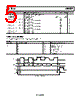
️· Timing Diagram: Referenced (Figure 1) for visual representation.
5. Charge Pump Current Setting
️· DB10, DB11 and DB18 of Register 4 are used to control the charge pump current.
️· The nominal charge pump current can be externally tweaked using a resistor to the RSET pin.
Important Considerations & Missing Information
️· Full Datasheet: This is an excerpt. A complete datasheet would contain much more information (typical performance, AC characteristics, application circuits, package information, etc.).
️· Register Descriptions: References to "Register 4" suggest that the device is configurable using registers. The datasheet excerpt doesn't provide descriptions of these registers.
️· Application Notes: Likely, there are application notes describing how to properly use this device in a system.
1. General Overview & Warnings
️· Device: ADRF6807 (likely a high-frequency/RF integrated circuit - based on the terminology)
️· Absolute Maximum Ratings: These are critical limits. Exceeding them can cause permanent damage. Important values include voltage ranges, junction temperature, and operating/storage temperatures.
️· ESD Caution: Electrostatic Discharge can harm the device. Handle with appropriate precautions.
2. Pin Configuration & Functions
️· Pinout Diagram: Included, showing pin numbers and their abbreviations (e.g., VCC1, RFIN, GND).
️· Pin Descriptions Table: A crucial table describing the function of *each* pin. Key pins and functions include:
- VCC1, VCC2, VCCBB, VCCRF, VCCLO: Power supply pins (different voltage levels).
- RSET: Charge Pump Current Setting.
- REFIN: Reference Input.
- RFIN, RFIP: RF input pins.
- VOCM: Output Common Mode voltage
- CPOUT: Charge Pump output – connects to VTUNE through a loop filter.
3. Electrical Characteristics (Implied, not fully detailed)
️· The data sheet excerpt implies a detailed electrical characteristic section is present elsewhere (not included in this snippet). This would include typical voltages, currents, gain, noise figure, etc.
4. Timing Characteristics (Table 2)
️· Purpose: Defines timing relationships for data signals.
️· Key Parameters:
- `t1` (LE setup time)
- `t2` (DATA to CLK setup time)
- `t3` (DATA to CLK hold time)
- `t4` (CLK high duration)
- and others related to CLK, DATA, and LE signals.
️· Timing Diagram: Referenced (Figure 1) for visual representation.
5. Charge Pump Current Setting
️· DB10, DB11 and DB18 of Register 4 are used to control the charge pump current.
️· The nominal charge pump current can be externally tweaked using a resistor to the RSET pin.
Important Considerations & Missing Information
️· Full Datasheet: This is an excerpt. A complete datasheet would contain much more information (typical performance, AC characteristics, application circuits, package information, etc.).
️· Register Descriptions: References to "Register 4" suggest that the device is configurable using registers. The datasheet excerpt doesn't provide descriptions of these registers.
️· Application Notes: Likely, there are application notes describing how to properly use this device in a system.
| Part No. | ADRF6807 |
| Manufacturer | AD |
| Size | 1,004 Kbytes |
| Pages | 36 pages |
| Description | 700 MHz to 1050 MHz Quadrature |
| Вашему бизинису помогли Аллдатащит? [ DONATE ] |
Что такое Аллдатащит | реклама | контакт | Конфиденциальность | Ссылка на техническое описание | обмен ссыками | поиск по производителю All Rights Reserved©Alldatasheet.com |
| Russian : Alldatasheetru.com | Korean : Alldatasheet.co.kr | Spanish : Alldatasheet.es | French : Alldatasheet.fr | Italian : Alldatasheetit.com Portuguese : Alldatasheetpt.com | Polish : Alldatasheet.pl | Vietnamese : Alldatasheet.vn Indian : Alldatasheet.in | Mexican : Alldatasheet.com.mx | British : Alldatasheet.co.uk | New Zealand : Alldatasheet.co.nz |
|
Family Site : ic2ic.com |
icmetro.com |
 Russian ▼
  English
 Chinese
 German
 Japanese
 Korean
 Spanish
 French
 Italian
 Portuguese
 Polish
 Vietnamese
 Indian
 Mexican
 British
 New Zealand