 |
поискавой системы для электроныых деталей |
|
|
поискавой системы для электроныых деталей |
|
The question interval is too short.
Please try again in a few seconds.

Hello, Please ask a question about V61C31161024 Datasheet
# Example questions:
➢ What is the minimum write pulse width (twp) for the -10 speed grade?
➢ In the 'read cycle 1' waveform, what signal must be held high to enable the read operation?
➢ What are the two package types available for this memory chip?
| Part No. | V61C31161024 |
| Manufacturer | MOSEL |
| Size | 83 Kbytes |
| Pages | 10 pages |
| Description | 64K x 16 HIGH SPEED STATIC RAM |




1. Chip Identification & Description:
️· Part Number: V61C31161024
️· Type: Synchronous Static RAM (SSRAM) - This means it's RAM that operates synchronously with a clock signal and uses static (not dynamic) memory cells.
2. Key Features (Implied - from the info presented):
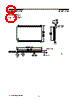
️· Package: Available in a 44-pin 400 mil TSOP-II package. The document includes a diagram of this package.
️· Synchronous Operation: Requires a clock signal for proper function.
️· Multiple Control Signals: Uses control signals like CE (Chip Enable), WE (Write Enable), OE (Output Enable), UBE, and LBE to manage read/write operations. These signals are crucial for timing and bus contention avoidance.
3. Electrical Characteristics:
️· Supply Voltage: (Not explicitly stated, but likely 3.3V or 5V – standard for SSRAMs. This needs confirmation from other sources.)
️· Operating Temperature: (Not specified but is standard for RAM)
️· Timing Parameters: The datasheet provides a table of numerous timing parameters. These are *critical* for correctly operating the chip. Key elements include:
- Read Cycle Time (tRC): The minimum time required to complete a read operation. (Ranges from 10ns to 15ns, depending on the operating conditions.)
- Write Cycle Time (tWC): The minimum time required to complete a write operation. (Ranges from 10ns to 15ns, depending on the operating conditions.)
- Setup and Hold Times: Critical for ensuring data is properly latched during read/write cycles.
- CE, WE, OE timing: Specific timing relationships between these control signals are defined.
️· Control Signals and Operation:
- CE (Chip Enable): Activates the memory.
- WE (Write Enable): Enables writing data into the memory.
- OE (Output Enable): Enables reading data from the memory.
- UBE, LBE: These signals are likely used for more advanced memory organization or control schemes (specific function not fully clear from this datasheet excerpt).
4. Timing Diagrams (Read/Write Cycles):
️· The datasheet includes detailed timing diagrams for both Read and Write operations. These diagrams are *essential* for understanding the correct sequence of control signals and their relationship to the clock signal. The diagrams illustrate the required timing for setup and hold times, and the impact of CE, WE, and OE signals.
- Read Cycle 1/2/3: Shows different ways to initiate a read operation.
- Write Cycle 1/2: Shows different ways to initiate a write operation.
️· The diagrams clarify the use of control signals and their critical relationships to timing parameters.
5. Package Information:
️· Detailed measurements and specifications for the 44-pin TSOP-II package.
Important Notes & What's Missing:
️· Supply Voltage: This is a critical parameter missing from this excerpt. You *must* find this information elsewhere.
️· Memory Organization: The datasheet doesn’s specify the memory's capacity.
️· Detailed Function of UBE and LBE: The exact purpose of these signals is not fully explained.
️· Detailed Electrical Characteristics: There’s a significant amount of electrical characteristics information not present in this excerpt (e.g., input/output voltage levels, power consumption, etc.).
To use this information effectively, you would need:
1. The full datasheet: This excerpt is just a portion of a much larger document.
2. A system design perspective: You need to understand how the memory will be integrated into a larger system to determine appropriate operating conditions and timing constraints.
3. Simulation and Verification: It’s highly recommended to simulate the memory's operation with the rest of the system.
1. Chip Identification & Description:
️· Part Number: V61C31161024
️· Type: Synchronous Static RAM (SSRAM) - This means it's RAM that operates synchronously with a clock signal and uses static (not dynamic) memory cells.
2. Key Features (Implied - from the info presented):
️· Package: Available in a 44-pin 400 mil TSOP-II package. The document includes a diagram of this package.
️· Synchronous Operation: Requires a clock signal for proper function.
️· Multiple Control Signals: Uses control signals like CE (Chip Enable), WE (Write Enable), OE (Output Enable), UBE, and LBE to manage read/write operations. These signals are crucial for timing and bus contention avoidance.
3. Electrical Characteristics:
️· Supply Voltage: (Not explicitly stated, but likely 3.3V or 5V – standard for SSRAMs. This needs confirmation from other sources.)
️· Operating Temperature: (Not specified but is standard for RAM)
️· Timing Parameters: The datasheet provides a table of numerous timing parameters. These are *critical* for correctly operating the chip. Key elements include:
- Read Cycle Time (tRC): The minimum time required to complete a read operation. (Ranges from 10ns to 15ns, depending on the operating conditions.)
- Write Cycle Time (tWC): The minimum time required to complete a write operation. (Ranges from 10ns to 15ns, depending on the operating conditions.)
- Setup and Hold Times: Critical for ensuring data is properly latched during read/write cycles.
- CE, WE, OE timing: Specific timing relationships between these control signals are defined.
️· Control Signals and Operation:
- CE (Chip Enable): Activates the memory.
- WE (Write Enable): Enables writing data into the memory.
- OE (Output Enable): Enables reading data from the memory.
- UBE, LBE: These signals are likely used for more advanced memory organization or control schemes (specific function not fully clear from this datasheet excerpt).
4. Timing Diagrams (Read/Write Cycles):
️· The datasheet includes detailed timing diagrams for both Read and Write operations. These diagrams are *essential* for understanding the correct sequence of control signals and their relationship to the clock signal. The diagrams illustrate the required timing for setup and hold times, and the impact of CE, WE, and OE signals.
- Read Cycle 1/2/3: Shows different ways to initiate a read operation.
- Write Cycle 1/2: Shows different ways to initiate a write operation.
️· The diagrams clarify the use of control signals and their critical relationships to timing parameters.
5. Package Information:
️· Detailed measurements and specifications for the 44-pin TSOP-II package.
Important Notes & What's Missing:
️· Supply Voltage: This is a critical parameter missing from this excerpt. You *must* find this information elsewhere.
️· Memory Organization: The datasheet doesn’s specify the memory's capacity.
️· Detailed Function of UBE and LBE: The exact purpose of these signals is not fully explained.
️· Detailed Electrical Characteristics: There’s a significant amount of electrical characteristics information not present in this excerpt (e.g., input/output voltage levels, power consumption, etc.).
To use this information effectively, you would need:
1. The full datasheet: This excerpt is just a portion of a much larger document.
2. A system design perspective: You need to understand how the memory will be integrated into a larger system to determine appropriate operating conditions and timing constraints.
3. Simulation and Verification: It’s highly recommended to simulate the memory's operation with the rest of the system.
| Part No. | V61C31161024 |
| Manufacturer | MOSEL |
| Size | 83 Kbytes |
| Pages | 10 pages |
| Description | 64K x 16 HIGH SPEED STATIC RAM |
| Вашему бизинису помогли Аллдатащит? [ DONATE ] |
Что такое Аллдатащит | реклама | контакт | Конфиденциальность | Ссылка на техническое описание | обмен ссыками | поиск по производителю All Rights Reserved©Alldatasheet.com |
| Russian : Alldatasheetru.com | Korean : Alldatasheet.co.kr | Spanish : Alldatasheet.es | French : Alldatasheet.fr | Italian : Alldatasheetit.com Portuguese : Alldatasheetpt.com | Polish : Alldatasheet.pl | Vietnamese : Alldatasheet.vn Indian : Alldatasheet.in | Mexican : Alldatasheet.com.mx | British : Alldatasheet.co.uk | New Zealand : Alldatasheet.co.nz |
|
Family Site : ic2ic.com |
icmetro.com |
 Russian ▼
  English
 Chinese
 German
 Japanese
 Korean
 Spanish
 French
 Italian
 Portuguese
 Polish
 Vietnamese
 Indian
 Mexican
 British
 New Zealand