 |
поискавой системы для электроныых деталей |
|
|
поискавой системы для электроныых деталей |
|
The question interval is too short.
Please try again in a few seconds.

Hello, Please ask a question about 24LC512-E/MFG Datasheet
# Example questions:
➢ What is the primary function of the 'acknowledge polling' feature?
➢ Describe the difference between a 'byte write' and a 'page write' operation in the context of this device.
➢ Explain how the wp (write protection) pin functions and under what condition it allows writing to the device's memory.
| Part No. | 24LC512-E/MFG |
| Manufacturer | MICROCHIP |
| Size | 490 Kbytes |
| Pages | 26 pages |
| Description | 512K I2C??CMOS Serial EEPROM |


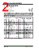


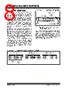

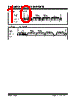


1. General Device Information (24XX512)
️· Type: EEPROM (Electrically Erasable Programmable Read-Only Memory). This is non-volatile memory, meaning it retains data even when power is removed.
️· Capacity: The specific capacity is not directly stated, but the address range (0000-FFFF) implies a 16-bit address space, which equates to 64KB (65536 bytes).
️· Addressing: Uses a 2-wire serial interface (I2C compatible).
️· Write Protection: The WP (Write Protect) pin allows the user to disable writing to the entire memory array when tied to VCC.
2. Serial Bus Communication
️· Data Transfer: Relies on a serial data transfer protocol. Data is transmitted bit by bit.
️· Control Byte: The first byte received by the slave device (24XX512) is a control byte.
- Format: `S | 1 | 0 | 1 | 0 | A2 | A1 | A0 | R/W | ACK`
■ `S`: Start bit
■ `1 0 1 0`: Device type identifier ('1010' binary)
■ `A2, A1, A0`: Chip Select bits (used for multiple devices on the same bus)
■ `R/W`: Read/Write control bit (0 for Write, 1 for Read)
■ `ACK`: Acknowledge bit (sent by the slave)
️· Addressing: Uses three chip select bits (A2, A1, A0) to address multiple devices on the same bus.
️· Acknowledge (ACK): The slave device (24XX512) generates an acknowledge signal after receiving each byte. This confirms successful receipt. The master generates an extra clock pulse for this ACK.
️· Read/Write operations: Acknowledge bit determines the operation.
3. Write Operations
️· Byte Write:
- A series of bytes are sent, followed by a Stop condition.
- Internal write cycle initiates after the Stop condition.
️· Page Write:
- A faster write method for writing multiple bytes sequentially.
- The master sends a control byte, address byte, and initial data byte. Then transmits up to 127 more bytes. After the master sends a Stop, an internal write cycle initiates.
️· Write Protection: The WP pin enables write protection of the entire memory.
4. Acknowledge Polling
️· Purpose: To determine when a write cycle is complete. This helps optimize bus throughput.
️· Method: The master sends a start condition followed by a write control byte. If a successful ack is returned, it indicates that the previous write cycle is finished.
5. Key Points & Considerations
️· Contiguous Addressing: It's *not* possible to sequentially read across multiple devices on the bus.
️· Write Cycle Time: The document does not specify the exact write cycle time, but it's an important factor in application design.
️· Power Supply: Ensure appropriate power supply voltages are used.
️· Timing: Adhere to the specified timing parameters for reliable communication.
In essence, the document describes a 64KB EEPROM that uses a serial communication protocol, allowing data to be written, read, and erased electronically. The document also explains how to efficiently manage the communication process and write protection functionality.
1. General Device Information (24XX512)
️· Type: EEPROM (Electrically Erasable Programmable Read-Only Memory). This is non-volatile memory, meaning it retains data even when power is removed.
️· Capacity: The specific capacity is not directly stated, but the address range (0000-FFFF) implies a 16-bit address space, which equates to 64KB (65536 bytes).
️· Addressing: Uses a 2-wire serial interface (I2C compatible).
️· Write Protection: The WP (Write Protect) pin allows the user to disable writing to the entire memory array when tied to VCC.
2. Serial Bus Communication
️· Data Transfer: Relies on a serial data transfer protocol. Data is transmitted bit by bit.
️· Control Byte: The first byte received by the slave device (24XX512) is a control byte.
- Format: `S | 1 | 0 | 1 | 0 | A2 | A1 | A0 | R/W | ACK`
■ `S`: Start bit
■ `1 0 1 0`: Device type identifier ('1010' binary)
■ `A2, A1, A0`: Chip Select bits (used for multiple devices on the same bus)
■ `R/W`: Read/Write control bit (0 for Write, 1 for Read)
■ `ACK`: Acknowledge bit (sent by the slave)
️· Addressing: Uses three chip select bits (A2, A1, A0) to address multiple devices on the same bus.
️· Acknowledge (ACK): The slave device (24XX512) generates an acknowledge signal after receiving each byte. This confirms successful receipt. The master generates an extra clock pulse for this ACK.
️· Read/Write operations: Acknowledge bit determines the operation.
3. Write Operations
️· Byte Write:
- A series of bytes are sent, followed by a Stop condition.
- Internal write cycle initiates after the Stop condition.
️· Page Write:
- A faster write method for writing multiple bytes sequentially.
- The master sends a control byte, address byte, and initial data byte. Then transmits up to 127 more bytes. After the master sends a Stop, an internal write cycle initiates.
️· Write Protection: The WP pin enables write protection of the entire memory.
4. Acknowledge Polling
️· Purpose: To determine when a write cycle is complete. This helps optimize bus throughput.
️· Method: The master sends a start condition followed by a write control byte. If a successful ack is returned, it indicates that the previous write cycle is finished.
5. Key Points & Considerations
️· Contiguous Addressing: It's *not* possible to sequentially read across multiple devices on the bus.
️· Write Cycle Time: The document does not specify the exact write cycle time, but it's an important factor in application design.
️· Power Supply: Ensure appropriate power supply voltages are used.
️· Timing: Adhere to the specified timing parameters for reliable communication.
In essence, the document describes a 64KB EEPROM that uses a serial communication protocol, allowing data to be written, read, and erased electronically. The document also explains how to efficiently manage the communication process and write protection functionality.
| Part No. | 24LC512-E/MFG |
| Manufacturer | MICROCHIP |
| Size | 490 Kbytes |
| Pages | 26 pages |
| Description | 512K I2C??CMOS Serial EEPROM |
| Вашему бизинису помогли Аллдатащит? [ DONATE ] |
Что такое Аллдатащит | реклама | контакт | Конфиденциальность | Ссылка на техническое описание | обмен ссыками | поиск по производителю All Rights Reserved©Alldatasheet.com |
| Russian : Alldatasheetru.com | Korean : Alldatasheet.co.kr | Spanish : Alldatasheet.es | French : Alldatasheet.fr | Italian : Alldatasheetit.com Portuguese : Alldatasheetpt.com | Polish : Alldatasheet.pl | Vietnamese : Alldatasheet.vn Indian : Alldatasheet.in | Mexican : Alldatasheet.com.mx | British : Alldatasheet.co.uk | New Zealand : Alldatasheet.co.nz |
|
Family Site : ic2ic.com |
icmetro.com |
 Russian ▼
  English
 Chinese
 German
 Japanese
 Korean
 Spanish
 French
 Italian
 Portuguese
 Polish
 Vietnamese
 Indian
 Mexican
 British
 New Zealand